Why in News?
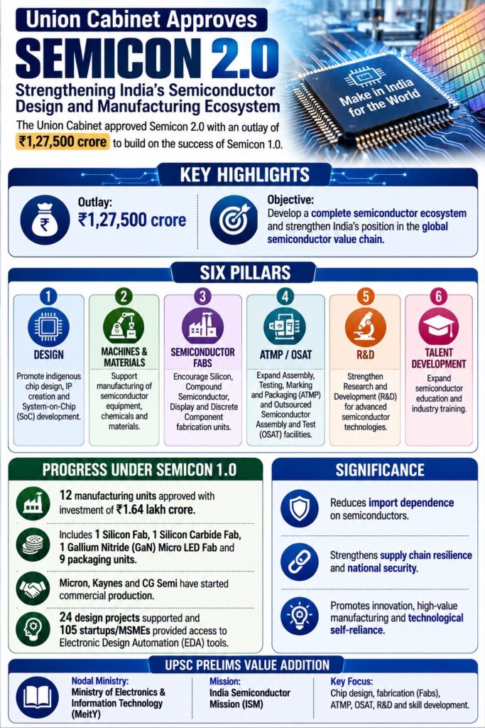
The Union Cabinet approved Semicon 2.0 with an outlay of ₹1,27,500 crore to strengthen India’s semiconductor design and manufacturing ecosystem after the success of Semicon 1.0.
Key Highlights
- Outlay: ₹1,27,500 crore.
- Objective: Develop a complete semiconductor ecosystem and strengthen India’s position in the global semiconductor value chain.
Six Pillars
- Design: Promote indigenous chip design, Intellectual Property (IP) creation and System-on-Chip (SoC) development.
- Machines & Materials: Support manufacturing of semiconductor equipment, chemicals and materials.
- Semiconductor Fabs: Encourage Silicon, Compound Semiconductor, Display and Discrete Component fabrication units.
- ATMP/OSAT: Expand Assembly, Testing, Marking and Packaging (ATMP) and Outsourced Semiconductor Assembly and Test (OSAT) facilities.
- R&D: Strengthen Research and Development (R&D) for advanced semiconductor technologies.
- Talent Development: Expand semiconductor education and industry training.
Progress under Semicon 1.0
- 12 manufacturing units approved with investment of ₹1.64 lakh crore.
- Includes 1 Silicon Fab, 1 Silicon Carbide Fab, 1 Gallium Nitride (GaN) Micro LED Fab and 9 packaging units.
- Micron, Kaynes and CG Semi have started commercial production.
- 24 design projects supported and 105 startups/MSMEs provided access to Electronic Design Automation (EDA) tools.
Significance
- Reduces import dependence on semiconductors.
- Strengthens supply chain resilience and national security.
- Promotes innovation, high-value manufacturing and technological self-reliance.
Prelims Pointer
- Nodal Ministry: Ministry of Electronics & Information Technology (MeitY)
- Mission: India Semiconductor Mission (ISM)
- Key Focus: Chip design, fabrication (Fabs), ATMP, OSAT, R&D and skill development.